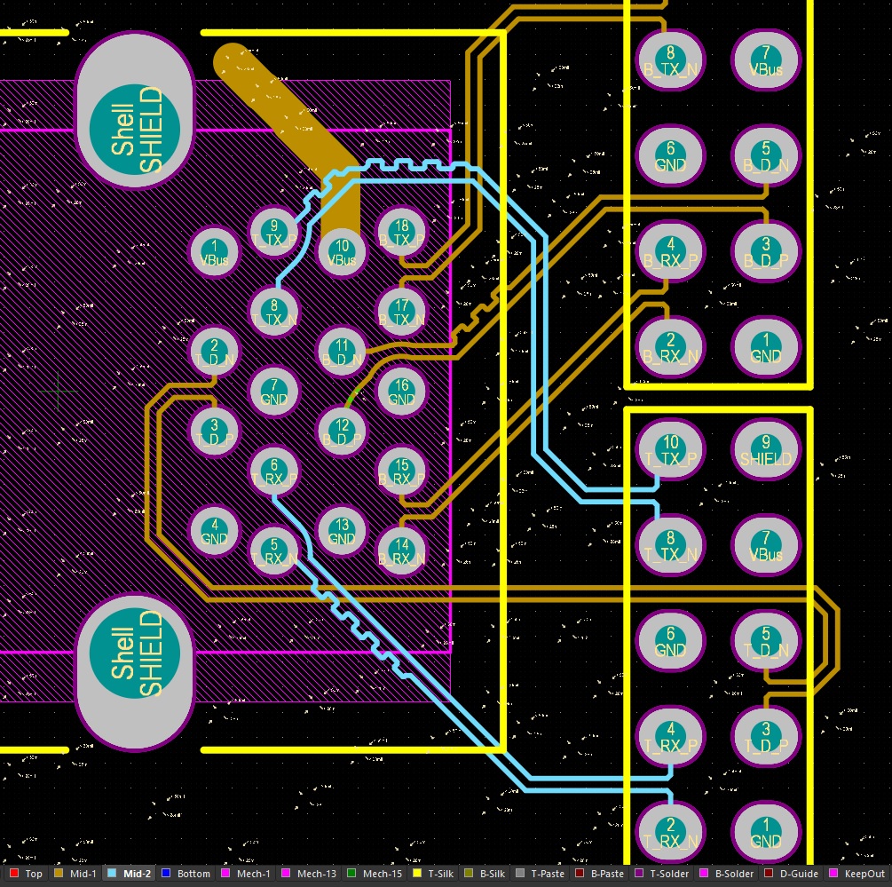
Differential pair routing is a critical issue in PCB design. If the differential pair signal is high speed signal like USB 2.0, USB 3.0 or HDMI then PCB routing is harder than lower speed signals like RS485, CAN or similar.
In this tutorial you are going to get how to set up schematic, PCB and design rules to route high speed differential pair signals. It should be known that the most important point is line impedance and what are you going to read in this tutorial, it is all related to impedance.
Design/Routing Steps:
- Read design notes, guides and technical papers / Analysis
- Set net as differential pair lines / Schematic
- Setup layer stack for impedance calculation / Layer Stack Manager
- Define net(s) for specific rule definition / PCB -> Net
- Setup rule for differential pair routing / Rules
- Setup rule for length tuning / Rules
Analysis: It is best if you read and understand what you are dealing with. What are potential problems and critical points. If you are being prepared for USB 3.x or HDMI here are some great documents from Texas Instruments and Cypress Semiconductor.
- High-Speed Interface Layout Guidelines – Texas
- USB 3.x Board Design and Layout Guidelines – Texas
- SuperSpeed USB Design Guidelines – Intel / Cypress
- HDMI Design Guide – Texas
end of Part 1, Wait for next